The PXB accepts binary data formatted into a binary I/Q file. The I/Q file contains the interleaved I and Q data points (signed 16-bit integers for each I and Q data point). Each I/Q point equals one waveform point. This topic explains the necessary components and formatting of the binary data, which uses ones and zeros to represent a value.
Binary data uses the base-two number system. The location of each bit
within the data represents a value that uses base two raised to a power
(2n-1). The
exponent is
1101 = (1 X 23) + (1 X 22) + (0 X 21) + (1 X 20)
= (1 X 8) + (1 X 4) + (0 X 2) + (1 X 1)
= 13 (decimal value)
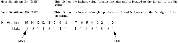
Notice that the exponent identifies the bit position within the data, and we read the data from right to left.
The PXB accepts data in the form of bytes. Bytes are groups of eight bits:
01101110 = (0 X 27) + (1 X 26) + (1 X 25) + (0 X 24) +(1 X 23) + (1 X 22) + (1 X 21) + (0 X 20) = 110 (decimal value)
The maximum value for a single unsigned byte is 255 (11111111 or
01101110 10110011= 28339 (decimal value)
For I and Q data, the PXB uses two bytes to represent an integer value.
The maximum value for two unsigned bytes is 65535. Since binary strings
lengthen as the value increases, it is common to show binary values using
hexadecimal (hex) values (base 16), which are shorter. The value 65535
in hex is
|
1 = 0001 |
2 = 0010 |
3 = 0011 |
4 = 0100 |
5 = 0101 |
|
6 = 0110 |
7 = 0111 |
8 = 1000 |
9 = 1001 |
A = 1010 |
|
B = 1011 |
C = 1100 |
D = 1101 |
E = 1110 |
F = 1111 |
Within groups (strings) of bits, we designate the order of the bits by identifying which bit has the highest value and which has the lowest value by its location in the bit string. The following is an example of this order.
Because we are using 2 bytes of data, the LSB appears in the second byte.
When you use multiple bytes (as required for the waveform data), you must identify their order. This is similar to identifying the order of bits by LSB and MSB. To identify byte order, use the terms little endian and big endian. These terms are used by designers of computer processors.
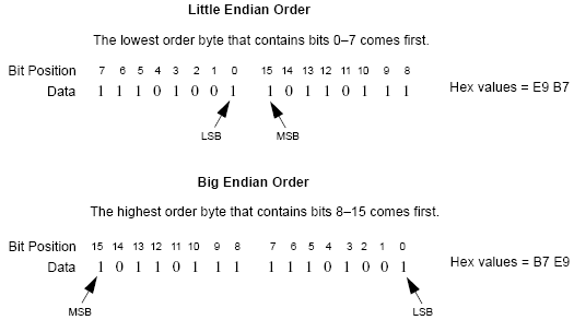
Notice in the previous figure that the LSB and MSB positioning changes with the byte order. In little endian order, the LSB and MSB are next to each other in the bit sequence.
|
|
For I/Q data downloads, the PXB accepts Big Endian order by default. Use the Endianess setting ([:SOURce]:RADio[1]2|3|4|5|6:ARB:FORMat:BORDer NORMal|SWAPped) to swap the byte order to Little Endian. For each I/Q data point, the PXB uses four bytes (two integer values), two bytes for the I point and two bytes for the Q point. |
The byte order, little endian or big endian, depends on the type of
processor used with your development platform. Intel© processors and its
clones use little endian. Sun™ and Motorola processors use big endian.
The Apple
|
|
Even though the PXB processor uses Little Endian, the byte order may be swapped internally for use on the baseband. Big endian is also used by the MXG, ESG, and PSG signal generators. |
Development platforms include any product that creates and saves waveform
data to a file. This includes Agilent Technologies Advanced Design System
The byte order describes how the system processor stores integer values as binary data in memory. If you output data from a little endian system to a text file (ASCII text), the values are the same as viewed from a big endian system. The order only becomes important when you use the data in binary format, as is done when downloading data to the PXB.
While the processor used for waveform development determines the byte order, the recipient of the data may require the bytes in the reverse order. In this situation, you must reverse the byte order before downloading the data. This is commonly referred to as byte swapping. You can swap bytes programmatically. For the PXB, byte swapping is the method to change the byte order of little endian to big endian. For more information on little endian and big endian order, see Little Endian and Big Endian (Byte Order).
The following figure shows the concept of byte swapping for the PXB. Remember that we can represent data in hex format (4 bits per hex value), so each byte (8 bits) in the figure shows two example hex values.

To correctly swap bytes, you must group the data to maintain the I and Q values. One common method is to break the two-byte integer into one-byte character values (0–255). Character values use 8 bits (1 byte) to identify a character. Remember that the maximum unsigned 8-bit value is 255 (28 – 1). Changing the data into character codes groups the data into bytes. The next step is to swap the bytes to align with big endian order.
The PXB uses a 16-bit DAC (digital-to-analog convertor) to process each of the 2-byte integer values for the I and Q data points. The DAC determines the range of input values required from the I/Q data. Remember that with 16 bits we have a range of 0–65535, but the PXB divides this range between positive and negative values:
32767 = positive full scale output
0 = 0 volts
−32768 = negative full scale output
Because the DAC’s range uses both positive and negative values, the PXB requires signed input values. The following list illustrates the DAC’s input value range.
|
Voltage Input Range |
|
|
1.0 |
32767 |
|
0.0 |
0 |
|
–1.0 |
–32767 |
Notice that it takes only 15 bits (215)
to reach the
The PXB uses an interpolation algorithm (sampling between the I/Q data points) when reconstructing the waveform. For common waveforms, this interpolation can cause overshoot, which may exceed the limits of the signal process path’s internal number representation, causing arithmetic overload. Because of the interpolation, the error condition can occur even when all the I and Q values are within the DAC input range. To avoid the DAC over- range problem, you must scale (reduce) the I and Q input values, so that any overshoot remains within the DAC range.
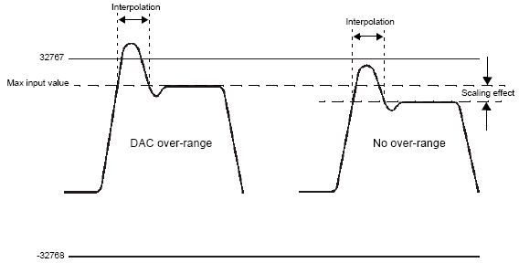
There is no single scaling value that is optimal for all waveforms. To achieve the maximum dynamic range, select the largest scaling value that does not result in a DAC over- range error. There are two ways to scale the I/Q data:
Reduce the input values for the DAC.
Use the SCPI command [:SOURce]:RADio[1]2|3|4:ARB:RSCaling <val> to set the waveform amplitude as a percentage of full scale.
|
|
The PXB factory preset for scaling is 70% (–3 dB) in baseband and 100% in the output I/O. If you reduce the DAC input values, ensure that you set the PXB scaling (CONTrol:IO[1]2|3|4:OUTPut:RSCaling) to an appropriate setting that accounts for the reduced values. |
The PXB requires signed values for the input data. For binary data, two’s complement is a way to represent positive and negative values. The most significant bit (MSB) determines the sign.
0 equals a positive value (01011011 = 91 decimal)
1 equals a negative value (10100101 =
Like decimal values, if you sum the binary positive and negative values, you get zero. The one difference with binary values is that you have a carry, which is ignored. The following shows how to calculate the two’s complement using 16 bits. The process is the same for both positive and negative values.
Convert the decimal value to binary.
23710 = 01011100 10011110
Notice that 15 bits (0-14) determine the value and bit 16 (MSB) indicates a positive value. Invert the bits (1 becomes 0 and 0 becomes 1).
10100011 01100001
Add one to the inverted bits. Adding one makes it a two’s complement of the original binary value.
10100011 01100001
+ 00000000 00000001
10100011 01100010
The MSB of the resultant is one, indicating a negative value (
01011100 10011110
+ 10100011 01100010
00000000
When you create the waveform data, the I and Q data points typically reside in separate arrays or files. The PXB requires a single I/Q file for waveform data playback. The process of interleaving creates a single array with alternating I and Q data points, with the Q data following the I data. This array is then downloaded to the PXB as a binary file. The interleaved file comprises the waveform data points where each set of data points, one I data point and one Q data point, represents one I/Q waveform sample.
The following figure illustrates interleaving I and Q data. Remember that it takes two bytes (16 bits) to represent one I or Q data point.
